Happy
Friday to everyone....! Hope everyone is having a great day today..
Lalala I seriously cant sleep and decided that I should update my
blog... hehe... I'm really trying hard and giving my very best to update
this blog so that I will not disappoint my followers and viewers....
>>> Specially just for my FANS.....! Enjoy today's entry and Hope you like it... :D <<<
Part 1: Assembled circuits
So far, I am done with the drilling
and soldering for the Blood Pressure PCB, but I still have trouble to
produce a good output with the BP board. So, it is still under further
construction and troubleshooting.... Secondly, I have also tried
combining all circuits that I have made into one combined/ single
unit..... refer Figure 1 :)

Figure 1: Combined schematic diagram
Just for an overall overview of the "Home Patient Monitor" project:
The main circuits used are:
1) PIC main board
2) Heart rate circuit using LDR
3) Blood pressure circuit (for signal filtering and amplification)
4) Body temperature circuit using LM35
5) Power supply for the PIC main board
6) Power supply for the DC motor
Others:
7) DC motor
8) Max232
9) Relay switch circuit
10) LCD
11) switch buttons (3 switches)
So
far, everything is done except for Blood Pressure circuit... I am still
troubleshooting the BP circuit as it does not work as it suppose to...
sob2 sad :( The BP circuit took a much longer time than expected. Once it is done, I will reveal the PCB board okay :) Now, lets look at the inputs and outputs circuit of this project.
The inputs are:
1) LM35
2) LDR
3) Blood pressure
The outputs are:
1) LCD
2) Computer monitor (Visual Basic)
This
week I emphasize work more on the BP circuit troubleshooting and the
construction of the MAX232 circuit for interfacing purposes.
Interfacing circuit used:
1) MAX232
2) USB converter cable

Figure 2: MAX232 pin configuration
- The MAX232 is an integrated circuit that converts signals from an RS-232 serial port to signals suitable for use in TTL compatible digital logic circuits. The MAX232 is a dual driver/receiver and typically converts the RX, TX, CTS and RTS signal.
- The drivers provide RS-232 voltage level outputs (approx. ± 7.5 V) from a single + 5 V supply via on-chip charge pumps and external capacitors. This makes it useful for implementing RS-232 in devices that otherwise do not need any voltages outside the 0 V to + 5 V range, as power supply design does not need to be made more complicated just for driving the RS-232 in this case.
- The receivers reduce RS-232 inputs (which may be as high as ± 25 V), to standard 5 V TTL levels. These receivers have a typical threshold of 1.3 V, and a typical hysteresis of 0.5 V.
- The later MAX232A is backwards compatible with the original MAX232 but may operate at higher baud rates and can use smaller external capacitors – 0.1 μF in place of the 1.0 μF capacitors used with the original device.
It is helpful to understand what occurs to the voltage levels. When a
MAX232 IC receives a TTL level to convert, it changes a TTL Logic 0 to
between +3 and +15 V, and changes TTL Logic 1 to between -3 to -15 V,
and vice versa for converting from RS232 to TTL. This can be confusing
when you realize that the RS232 Data Transmission voltages at a certain
logic state are opposite from the RS232 Control Line voltages at the
same logic state. To clarify the matter, see the table below. For more
information see RS-232 Voltage Levels.
| RS232 Line Type & Logic Leve | RS232 Voltage | TTL Voltage to/from MAX232 |
|---|---|---|
| Data Transmission (Rx/Tx) Logic 0 | +3 V to +15 V | 0 V |
| Data Transmission (Rx/Tx) Logic 1 | -3 V to -15 V | 5 V |
| Control Signals (RTS/CTS/DTR/DSR) Logic 0 | -3 V to -15 V | 5 V |
| Control Signals (RTS/CTS/DTR/DSR) Logic 1 | +3 V to +15 V | 0 V |
Source of refference http://en.wikipedia.org/wiki/MAX232
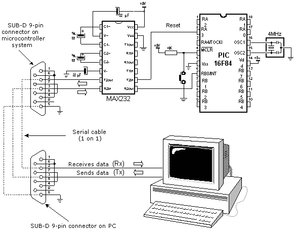
Figure 3: Connection flow
Part 3: MAX232 Construction
Below, I have attached the components used for the MAX232 circuit construction. Click here for the MAX232 datasheet. For better understanding refer the comparison of MAX220 to MAX249 family here.

Figure 4: Components used to make the MAX232 for interfacing circuit

Figure 5: Component placement on the PCB
As you can see the circuit requires alot of capacitors, this is simply for the noise filtration purposes. Hehe :p

Figure 6: Component soldering
So, there it is, TADAAAAA......my finished MAX232 circuit...!! That's it for today... Hope u guys enjoy my entry for today.... Wait for my next post okay next week k.... Gonna miss u all.... <3
Bubye peeps.... ('.' )v
[][][][][][][][][][][][][][][][][][][][][][][][]][][][][][][][][]
[][][][][][][][][][][][][][][][][][][][][][][][]][][][][][][][][][][][][][][][][][][][][][][][][][][][][][][][][][][][]
[][][][][][][][][][][][][][][][][][][][][][][][][][][][][][][][][][][][][][][][][][][][][][][][][][][][][][][][][][][][]
Quote of the day....!
Face what you think you believe and you will be surprised. ~William Hale White
[][][][][][][][][][][][][][][][][][][][][][][][][][][][][][][][][][][][][][][][][][][][][][][][][][][][][][][][][][][][]
[][][][][][][][][][][][][][][][][][][][][][][][]][][][][][][][][][][][][][][][][][][][][][][][][][][][][][][][][][][][]
Regards,
Idriah Safriza ('.' )k
